Overview
This section consists of various projects, with a focus on technology applications, which demonstrate the advanced functionality of Meep and MPB. Refer to their homepages for an introduction to each software package including descriptions of features and Python user interface as well as tutorials demonstrating basic functionality. Each project consists of a Python simulation script, a shell script to run the simulation, and Python post-processing routines for visualizing the output. A version of this page is available for the Scheme user interface.- Meep Project #1 — Light-Extraction Efficiency of Organic Light Emitting Diodes (OLEDs)
- MPB Project #1 — Modes of Silicon on Insulator (SOI) Strip Waveguides
- Meep Project #2 — Optimizing Far-Field Radiated Power of SOI Bragg Grating Outcouplers
- MPB Project #2 — Band Gap of Photonic-Crystal Nanobeam Waveguide
- Meep Project #3 — Resonant Modes of a Photonic-Crystal Nanobeam Cavity
- Meep Project #4 — Near-Infrared Absorption Spectra of CMOS Image Sensors
- Meep Project #5 — Thermal Radiation Spectra of Plasmonic Metamaterials
- Meep Project #6 — Bidirectional Scattering Distribution Function (BSDF) of Asymmetric Gratings
Meep Project #1 — Light-Extraction Efficiency of Organic Light Emitting Diodes (OLEDs)
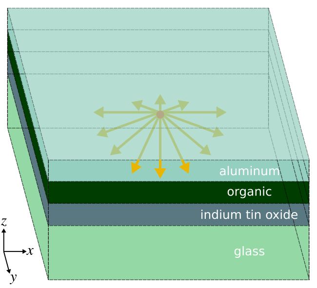
Organic light-emitting diodes (OLEDs) are being increasingly used in display applications involving mobile devices and televisions due to their higher contrast ratios, color uniformity, and wider viewing angle than liquid-crystal displays. One of the main limitations of OLED energy efficiency is the low light extraction from the device. In this example, we use Meep to compute the light-extraction efficiency of an OLED. This is based on results published in Applied Physics Letters, Vol. 106, No. 041111, 2015 (pdf). US Patent 9761842, related to this work, has been licensed by Universal Display Corporation (NASDAQ: OLED).A typical device structure for a bottom-emitting OLED is shown below. The device consists of a stack of four planar layers. The organic (ORG) layer is deposited on an indium tin oxide (ITO) coated glass substrate with an aluminum (Al) cathode layer on top. Electrons are injected into the organic layer from the Al cathode and holes from the ITO anode. These charge carriers form bound states called excitons which spontaneously recombine to emit photons. Light is extracted from the device through the transparent glass substrate. Some of the light, however, remains trapped within the device as (1) waveguide modes in the high-index ORG/ITO layers and (2) surface-plasmon polaritons (SPP) at the Al/ORG interface. These losses significantly reduce the external quantum efficiency (EQE) of OLEDs. We compute the fraction of the total power in each of these three device components for broadband emission from a white source spanning 400 to 800 nm. The results can be obtained using a single finite-difference time-domain (FDTD) simulation.
There are three key features involved in developing an accurate model. (1) Material Properties: The complex refractive index over the entire broadband spectrum must be imported for each material. This requires fitting the material data to a sum of Drude-Lorentzian susceptibility terms. In this example, we treat the glass, ITO, and organic as lossless since their absorption coefficient is small. The refractive index of Al can be obtained from Applied Optics, Vol. 37, pp. 5271-83, 1998. (2) Recombining Excitons as Light Source: An ensemble of spontaneously-recombining excitons produces incoherent emission. This can be modeled using a collection of point-dipole sources with random phase positioned within the organic layer. Given the stochastic nature of the sources, the results must be averaged using Monte-Carlo sampling. The number of samples must be large enough to ensure that the variance of the computed quantities is sufficiently small. (3) Flux Monitors: The total power separated into the three device components is computed using flux monitors. The size and position of these monitors must be chosen correctly to fully capture the relevant fields.
argparse module. This example also involves complex (cmath) and random (random) numbers.
import meep as mp
import cmath
import random
import argparse

def main(args):
We choose the unit length to be 1 μm. The choice of resolution requires a convergence test to determine a value suitable for a desired level of accuracy. This is particularly relevant in this example given the presence of the lossy-metal aluminum with its nanoscale skin depth as well as the flux monitors. Based on tests, the resolution is set to 100 pixels per μm which is equivalent to a pixel size of 10 nm.
resolution = 100 # pixels/um
We specify the frequency bounds of the Gaussian pulse using its minimum and maximum wavelengths in vacuum.
lambda_min = 0.4            # minimum source wavelength
lambda_max = 0.8            # maximum source wavelength
fmin = 1/lambda_max         # minimum source frequency
fmax = 1/lambda_min         # maximum source frequency
fcen = 0.5*(fmin+fmax)      # source frequency center
df = fmax-fmin              # source frequency width
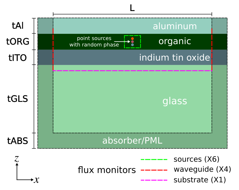
The thickness of each layer is a parameter. This is useful if we want to optimize the design. We use typical values for OLEDs. The length of the absorbing layer should be at least half the largest wavelength in the simulation to ensure negligible reflections. This is because incident waves are absorbed twice through a round-trip reflection from the hard-wall boundaries of the computational cell.
tABS = lambda_max           # absorber/PML thickness
tGLS = 1.0                  # glass thickness
tITO = 0.1                  # indium tin oxide thickness
tORG = 0.1                  # organic thickness
tAl = 0.1                   # aluminum thickness

# length of computational cell along Z
sz = tABS+tGLS+tITO+tORG+tAl
Since this is a 3d simulation, we also need to specify the length of the computational cell in the transverse directions X and Y. This is the length of the high-index organic/ITO waveguide. We choose a value of several wavelengths. The choice of the waveguide length has a direct impact on the results.
# length of non-absorbing region of computational cell in X and Y
L = args.L
sxy = L+2*tABS
cell_size = mp.Vector3(sxy,sxy,sz)
Overlapping the lossy-metal aluminum with a perfectly-matched layer (PML) sometimes leads to field instabilities due to backward-wave SPPs. Meep provides an alternative absorber which tends to be more stable. We use an absorber in the X and Y directions and a PML for the outgoing waves in the glass substrate. The metal cathode on top of the device either reflects or absorbs the incident light. No light is transmitted. Thus, we need a PML along just one side in the Z direction.
boundary_layers = [mp.Absorber(tABS, direction=mp.X),
                   mp.Absorber(tABS, direction=mp.Y),
                   mp.PML(tABS, direction=mp.Z, side=mp.High)]
Next, we define the material properties and set up the geometry consisting of the four-layer stack. Aluminum (Al) is imported from Meep's materials library.
ORG = mp.Medium(index=1.75)
ITO = mp.Medium(index=1.80)
GLS = mp.Medium(index=1.45)

from meep.materials import Al

geometry = [mp.Block(material=GLS, size=mp.Vector3(mp.inf,mp.inf,tABS+tGLS), center=mp.Vector3(0,0,0.5*sz-0.5*(tABS+tGLS))),
            mp.Block(material=ITO, size=mp.Vector3(mp.inf,mp.inf,tITO), center=mp.Vector3(0,0,0.5*sz-tABS-tGLS-0.5*tITO)),
            mp.Block(material=ORG, size=mp.Vector3(mp.inf,mp.inf,tORG), center=mp.Vector3(0,0,0.5*sz-tABS-tGLS-tITO-0.5*tORG)),
            mp.Block(material=Al, size=mp.Vector3(mp.inf,mp.inf,tAl), center=mp.Vector3(0,0,0.5*sz-tABS-tGLS-tITO-tORG-0.5*tAl))]
We use a set of point-dipole sources, each with random phase but fixed polarization, distributed along a line within the middle of the organic layer. The number of point sources is a parameter with a default of 10. The polarization of the source has an important effect on the results which we will investigate. Instead of using a random polarization, which would require multiple runs to obtain a statistical average, the sources can be separated into components which are parallel (directions X and Y) and perpendicular (Z) to the layers. Thus, we will need to do just two sets of simulations. These are averaged to obtain results for random polarization. We can also exploit the two mirror symmetry planes of the sources and the structure in order to reduce the size of the computation by a factor four. The phase of the mirror symmetry planes depends on the polarization of the source. Finally, since only the source and not the structure is being changed between runs, we can store the epsilon in the first run as an HDF5 file and load it back in during subsequent runs. This speeds up the calculation by forgoing subpixel smoothing which is time intensive. An input parameter load_structure specifies whether to load the structure from file or save the geometry to file.
# current-source component
if args.perp_dipole:
    src_cmpt = mp.Ez
    symmetries = [mp.Mirror(mp.X,+1), mp.Mirror(mp.Y,+1)]
else:
    src_cmpt = mp.Ex
    symmetries = [mp.Mirror(mp.X,-1), mp.Mirror(mp.Y,+1)]

num_src = 10                 # number of point sources
sources = [];
for n in range(1, num_src):
    sources.append(mp.Source(mp.GaussianSource(fcen, fwidth=df), component=src_cmpt,
                             center=mp.Vector3(0,0,0.5*sz-tABS-tGLS-tITO-0.4*tORG-0.2*tORG*n/num_src),
                             amplitude=cmath.exp(2*cmath.pi*random.random()*1j)))

if args.load_structure:
        epsilon_filename = 'oled_epsilon.h5'
        geometry = []
    else:
        epsilon_filename = ''
Three sets of flux monitors are required to capture the power in the sources, glass substrate, and high-index waveguide. We place a set of six flux planes along the sides of a box to enclose the sources. This is used to compute the total power in the device. These monitors must be placed entirely within the organic layer. One flux plane is required to compute the power in the glass substrate. Four flux planes are required to capture the total power of the modes in the high-index waveguide forming the organic/ITO layers. These modes are delocalized and extend slightly beyond these two layers. This requires the height of the flux planes to be larger than the combined thickness of the layers as shown in the figure above. Also, any component of the guided mode which extends into the aluminum will be absorbed due to screening effects of the charges in the metal. The longer the waveguide is made, the more these guided modes will be absorbed. This is why the length of the waveguide (L) should not be made so large that the waveguide component of the total power is zero.
sim = mp.Simulation(resolution=resolution,
                    cell_size=cell_size,
                    boundary_layers=boundary_layers,
                    geometry=geometry,
                    dimensions=3,
                    sources=sources,
                    force_complex_fields=True,
                    symmetries=symmetries)

# number of frequency bins for DFT fields
nfreq = 50

# surround source with a six-sided box of flux planes
srcbox_width = 0.05
srcbox_top = sim.add_flux(fcen, df, nfreq,
                          mp.FluxRegion(center=mp.Vector3(0,0,0.5*sz-tABS-tGLS),
                                        size=mp.Vector3(srcbox_width,srcbox_width,0), direction=mp.Z, weight=+1))
srcbox_bot = sim.add_flux(fcen, df, nfreq,
                          mp.FluxRegion(center=mp.Vector3(0,0,0.5*sz-tABS-tGLS-tITO-0.8*tORG),
                                        size=mp.Vector3(srcbox_width,srcbox_width,0), direction=mp.Z, weight=-1))
srcbox_xp = sim.add_flux(fcen, df, nfreq,
                         mp.FluxRegion(center=mp.Vector3(0.5*srcbox_width,0,0.5*sz-tABS-tGLS-0.5*(tITO+0.8*tORG)),
                                       size=mp.Vector3(0,srcbox_width,tITO+0.8*tORG), direction=mp.X, weight=+1))
srcbox_xm = sim.add_flux(fcen, df, nfreq,
                         mp.FluxRegion(center=mp.Vector3(-0.5*srcbox_width,0,0.5*sz-tABS-tGLS-0.5*(tITO+0.8*tORG)),
                                       size=mp.Vector3(0,srcbox_width,tITO+0.8*tORG), direction=mp.X, weight=-1))
srcbox_yp = sim.add_flux(fcen, df, nfreq,
                         mp.FluxRegion(center=mp.Vector3(0,0.5*srcbox_width,0.5*sz-tABS-tGLS-0.5*(tITO+0.8*tORG)),
                                       size=mp.Vector3(srcbox_width,0,tITO+0.8*tORG), direction=mp.Y, weight=+1))
srcbox_ym = sim.add_flux(fcen, df, nfreq,
                         mp.FluxRegion(center=mp.Vector3(0,-0.5*srcbox_width,0.5*sz-tABS-tGLS-0.5*(tITO+0.8*tORG)),
                                       size=mp.Vector3(srcbox_width,0,tITO+0.8*tORG), direction=mp.Y, weight=-1))

# padding for flux box to fully capture waveguide mode
fluxbox_dpad = 0.05

# upward flux into glass substrate
glass_flux = sim.add_flux(fcen, df, nfreq,
                          mp.FluxRegion(center=mp.Vector3(0,0,0.5*sz-tABS-(tGLS-fluxbox_dpad)),
                                        size = mp.Vector3(L,L,0), direction=mp.Z, weight=+1))

# surround ORG/ITO waveguide with four-sided box of flux planes
# NOTE: waveguide mode extends partially into Al cathode and glass substrate
wvgbox_xp = sim.add_flux(fcen, df, nfreq,
                         mp.FluxRegion(size=mp.Vector3(0,L,fluxbox_dpad+tITO+tORG+fluxbox_dpad), direction=mp.X,
                                       center=mp.Vector3(0.5*L,0,0.5*sz-tABS-tGLS-0.5*(tITO+tORG)), weight=+1))
wvgbox_xm = sim.add_flux(fcen, df, nfreq,
                         mp.FluxRegion(size=mp.Vector3(0,L,fluxbox_dpad+tITO+tORG+fluxbox_dpad), direction=mp.X,
                                       center=mp.Vector3(-0.5*L,0,0.5*sz-tABS-tGLS-0.5*(tITO+tORG)), weight=-1))
wvgbox_yp = sim.add_flux(fcen, df, nfreq,
                         mp.FluxRegion(size=mp.Vector3(L,0,fluxbox_dpad+tITO+tORG+fluxbox_dpad), direction=mp.Y,
                                       center=mp.Vector3(0,0.5*L,0.5*sz-tABS-tGLS-0.5*(tITO+tORG)), weight=+1))
wvgbox_ym = sim.add_flux(fcen, df, nfreq,
                         mp.FluxRegion(size=mp.Vector3(L,0,fluxbox_dpad+tITO+tORG+fluxbox_dpad), direction=mp.Y,
                                       center=mp.Vector3(0,-0.5*L,0.5*sz-tABS-tGLS-0.5*(tITO+tORG)), weight=-1))
Finally, with the structure and sources set up, the fields are time stepped until they have sufficiently decayed away due to absorption by the absorbing boundary layers or surface plasmons. Afterwards, the fractional power in each of the three device components is computed from the flux data. The results are written to standard output as four columns separated by commas. The first column is the wavelength.
sim.run(until_after_sources=mp.stop_when_fields_decayed(50, src_cmpt, mp.Vector3(0,0,0.5*sz-tABS-tGLS-tITO-0.5*tORG), 1e-8))

if not args.load_structure:
        sim.dump_structure('oled_epsilon.h5')

import numpy as np

flux_srcbox_top = np.asarray(mp.get_fluxes(srcbox_top))
flux_srcbox_bot = np.asarray(mp.get_fluxes(srcbox_bot))
flux_srcbox_xp = np.asarray(mp.get_fluxes(srcbox_xp))
flux_srcbox_xm = np.asarray(mp.get_fluxes(srcbox_xm))
flux_srcbox_yp = np.asarray(mp.get_fluxes(srcbox_yp))
flux_srcbox_ym = np.asarray(mp.get_fluxes(srcbox_ym))

flux_wvgbox_xp = np.asarray(mp.get_fluxes(wvgbox_xp))
flux_wvgbox_xm = np.asarray(mp.get_fluxes(wvgbox_xm))
flux_wvgbox_yp = np.asarray(mp.get_fluxes(wvgbox_yp))
flux_wvgbox_ym = np.asarray(mp.get_fluxes(wvgbox_ym))

flux_glass = np.asarray(mp.get_fluxes(glass_flux))

flux_total = flux_srcbox_top+flux_srcbox_bot+flux_srcbox_xp+flux_srcbox_xm+flux_srcbox_yp+flux_srcbox_ym
flux_waveguide = flux_wvgbox_xp+flux_wvgbox_xm+flux_wvgbox_yp+flux_wvgbox_ym

frac_glass = flux_glass/flux_total
frac_waveguide = flux_waveguide/flux_total
frac_aluminum = 1-frac_glass-frac_waveguide

freqs = np.asarray(mp.get_flux_freqs(glass_flux))
lambdas = 1/freqs
lambdas_linear = np.linspace(lambda_min,lambda_max,nfreq)

from scipy import interpolate

g_linear = interpolate.interp1d(lambdas,frac_glass,kind='cubic')
w_linear = interpolate.interp1d(lambdas,frac_waveguide,kind='cubic')
a_linear = interpolate.interp1d(lambdas,frac_aluminum,kind='cubic')
frac_glass_linear = g_linear(lambdas_linear)
frac_waveguide_linear = w_linear(lambdas_linear)
frac_aluminum_linear = a_linear(lambdas_linear)

for j in range(nfreq):
    print("data:, {:.4f}, {:.6f}, {:.6f}, {:.6f}".format(lambdas_linear[j],
                                                         frac_glass_linear[j],
                                                         frac_waveguide_linear[j],
                                                         frac_aluminum_linear[j]))
The last component of the script involves specifying the command-line parameters and their default values.
if __name__ == '__main__':
    parser = argparse.ArgumentParser()
    parser.add_argument('-L', type=float, default=4.0, help='length of OLED (default: 4.0 um)')
    parser.add_argument('--perp_dipole', action='store_true', help='perpendicular dipole (default: False)')
    parser.add_argument('--load_structure', action='store_true', help='load structure from HDF5 file? (default: False)')
    args = parser.parse_args()
    main(args)
We use the following Bash script to launch a parallel Meep simulation using 20 processors.
#!/bin/bash

mpirun -np 20 python3 -u oled_ext_eff.py -L $1 > oled-flux.out;
grep data: oled-flux.out |cut -d , -f2- > oled-flux.dat;
This script is executed from the shell terminal using a waveguide length (L) of 4.
chmod u+x run_oled_python.sh
nohup ./run_oled_python.sh 4 &> /dev/null &
This takes about 3 hours to run on an Intel Xeon 2.60 GHz machine. Once the simulation is complete, we plot its output using a Jupyter/IPython notebook. The total power in each device component is the sum of the relevant columns of the output.
import numpy as np
import matplotlib.pyplot as plt

f = np.genfromtxt("oled-flux.dat", delimiter=",")
lambdas = f[:,0]
glass = f[:,1]
waveguide = f[:,2]
aluminum = f[:,3]

plt.plot(lambdas,glass,'b-',label='glass')
plt.plot(lambdas,waveguide,'r-',label='organic + ITO')
plt.plot(lambdas,aluminum,'g-',label='aluminum')
plt.xlabel("wavelength (um)"); plt.ylabel("fraction of total power")
plt.axis([0.4, 0.8, 0, 1])
plt.xticks([t for t in np.arange(0.4,0.9,0.1)])
plt.legend(loc='upper right')
plt.show()

print("glass: {} (mean), {} (std. dev.)".format(np.mean(glass),np.std(glass)))
print("waveguide: {} (mean), {} (std. dev.)".format(np.mean(waveguide),np.std(waveguide)))
print("aluminum: {} (mean), {} (std. dev.)".format(np.mean(aluminum),np.std(aluminum)))
Files: Simulation Script, Shell Launch Script, Plot Results. [gzipped tarball]
MPB Project #1 — Modes of Silicon on Insulator (SOI) Strip Waveguides
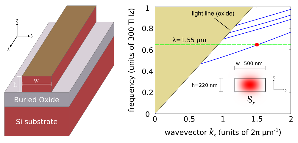
A key component of silicon photonic integrated circuits are waveguides. These devices are typically fabricated on silicon on insulator (SOI) wafers. Infrared light at 1.55 μm, the standard wavelength for telecommunications using silica fibers, is routed within the silicon using index guiding. We will use MPB to calculate the dispersion relation, also known as a band diagram, of these waveguide modes as shown in the right figure below. The focus is to design a waveguide which is single mode for the lowest band (i.e., the fundamental mode).The left figure shows the device structure. The silicon waveguide has a rectangular cross section with width w and height h. The buried oxide, typically silicon dioxide, is below the waveguide. A silicon substrate is beneath. No cladding is placed on top of the waveguide which is surrounded by air. The propagation axis is along X. This is the direction in which the waveguide is translationally invariant.
import meep as mp
from meep import mpb
We choose the unit length to be 1 μm. The resolution is 64 pixels per μm which is equivalent to a pixel size of approximately 16 nm. This is higher than necessary for accurate results given MPB's subpixel smoothing method.
resolution = 64 # pixels/um
The width and height of the waveguide are design parameters. Most SOI wafers have a 220 nm thick silicon layer which is used as the default value for the height. The default width is 500 nm.
w = 0.50  # Si width
h = 0.22  # Si height
This is a 3d calculation based on a 2d computational cell in Y and Z. The size of the computational cell needs to be large enough such that the fields are negligible at the edge of the computational cell. This ensures that MPB's periodic boundaries do not affect the results. Since the guided mode is localized within the silicon, the fields outside are exponentially decaying. There is a tradeoff to increasing the size of the computational cell: the size of the calculation also increases.
sc_y = 2  # supercell width
sc_z = 2  # supercell height

geometry_lattice = mp.Lattice(size=mp.Vector3(0,sc_y,sc_z))
Next, we specify the material properties of silicon and silicon dioxide. Silicon is lossless at 1.55 μm which is an important feature for these kinds of applications. The large refractive index contrast with silicon dioxide also produces strong mode confinement. Typical values for the refractive indicies are used as default.
Si = mp.Medium(index=3.45)
SiO2 = mp.Medium(index=1.45)
Since the oxide layer in which the waveguide modes are exponentially decaying is several microns in thickness, the fields are negligible at the silicon substrate. Thus, the substrate can be omitted from the device geometry. The geometry consists of just two objects: (1) a rectangular silicon waveguide at the center of the computational cell and (2) a planar oxide layer which fills the bottom half.
geometry = [mp.Block(size=mp.Vector3(mp.inf, w, h),
                     center=mp.Vector3(), material=Si),
            mp.Block(size=mp.Vector3(mp.inf, mp.inf, 0.5*(sc_z-h)),
                     center=mp.Vector3(z=0.25*(sc_z+h)), material=SiO2)]
The first four bands will be computed even though the single-mode property can be determined from only the first and second bands. The range of propagation wavevectors over which to compute the bands needs to be sufficiently large to contain modes at 1.55 μm. Finding suitable values typically requires a bit of trial and error.
num_bands = 4

num_k = 20
k_min = 0.1
k_max = 2.0
k_points = mp.interpolate(num_k, [mp.Vector3(k_min), mp.Vector3(k_max)])
We can now call the run function to compute the bands. The parity information in the Y direction for each mode is also output. This will help us identify properties of the modes since the fundamental mode has even symmetry.
ms = mpb.ModeSolver(geometry_lattice=geometry_lattice,
                    geometry=geometry,
                    k_points=k_points,
                    resolution=resolution,
                    num_bands=num_bands)

ms.run(mpb.display_yparities)
After the bands have been computed, we identify the mode(s) at 1.55 μm. This involves an inverse calculation where given the mode frequency (in vacuum), we compute its wavevector using MPB's built-in find-k routine. The Poynting vector along X of the fields is also output as an HDF5 file.
f_mode = 1/1.55   # frequency corresponding to 1.55 um
band_min = 1
band_max = 1
kdir = mp.Vector3(1)
tol = 1e-6
kmag_guess = f_mode*3.45
kmag_min = f_mode*0.1
kmag_max = f_mode*4.0

ms.find_k(mp.ODD_Y, f_mode, band_min, band_max, kdir, tol, kmag_guess,
          kmag_min, kmag_max, mpb.output_poynting_x, mpb.display_group_velocities)
This shell script is used to launch the simulation which takes a few seconds using a single Intel Xeon 2.60 GHz core. Afterwards, h5topng, part of the h5utils package, is used to generate a PNG image from the raw simulation data stored in the HDF5 file.
#!/bin/bash

python3 strip_wvg.py > strip_wvg_output.out;

grep freqs: strip_wvg_output.out |grep -v yoddfreqs |cut -d , -f3,7- |sed 1d > strip_wvg_bands.dat;

h5topng -o wvg_power.png -x 0 -d x.r -vZc bluered -C strip_wvg-epsilon.h5 strip_wvg-flux.v.k01.b01.x.yodd.h5;
Finally, we plot the results from the output and add the light line for the oxide.
from numpy import *
import matplotlib.pyplot as plt

f = genfromtxt("strip_wvg_bands.dat", delimiter=",")
plt.plot(f[:,0],f[:,1:],'b-',f[:,0],f[:,0]/1.45,'k-')
plt.xlabel("wavevector k_x (units of 2π μm^{-1})")
plt.ylabel("frequency (units of 300 THz)")
plt.axis([0,2,0,1])
plt.show()
This plot is shown in the right figure above. There is a single mode at 1.55 μm for the lowest band indicated with the dotted green line. The cutoff frequency of the second band lies above this mode frequency. The inset shows the Poynting vector along X (Sx). The antinode at the center of the waveguide verifies that this is the fundamental mode. This mode has a wavevector at 1.5192 μm-1 as calculated from the find-k routine.Files: Simulation Script, Shell Launch Script, Plot Results. [gzipped tarball]
Meep Project #2 — Optimizing Far-Field Radiated Power of SOI Bragg Grating Outcouplers
Coupling light into and out of silicon photonic integrated circuits is an important part of the overall device operation. For example, couplers are required when an external laser is used as the input light source or when the circuit signal must be transferred to an optical fiber for long-range transmission. This example involves designing a grating structure to outcouple light from an SOI strip waveguide and direct the beam into a given direction in the vacuum far field while minimizing losses due to reflection and scattering. We will use Meep to compute the far-field radiated power of the device and optimize the design by integrating Meep with NLopt, an open-source library for nonlinear optimization.The outcoupler design is based on Optics Express, Vol. 22, pp. 20652-62, 2014 which is a concentric Bragg grating with angled sides, shown in the figures below. The input port is an SOI strip waveguide which is connected to the Bragg grating.
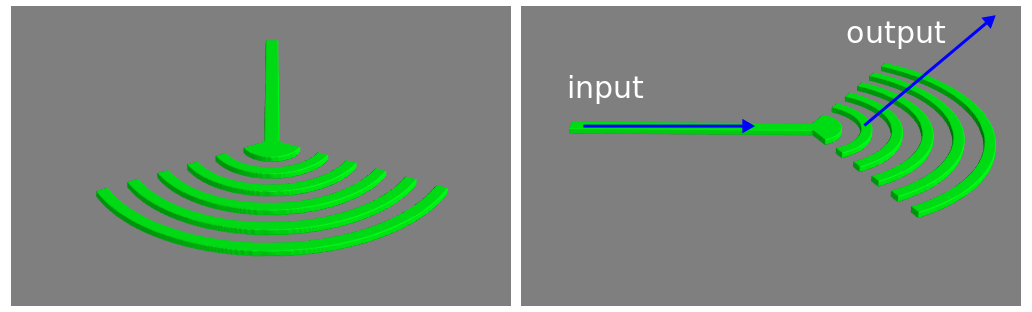
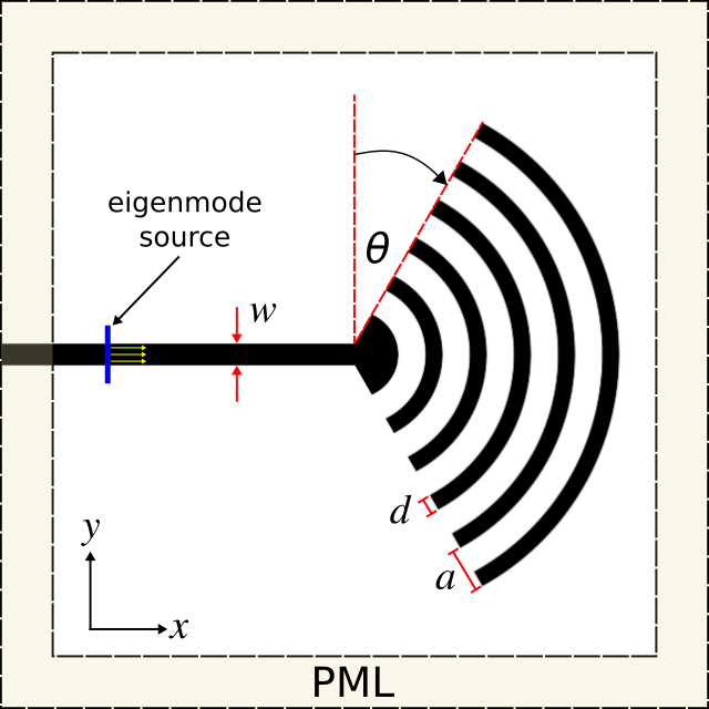
The figure below shows the device cross section in the XY plane of the computational cell. There are two parameters used to design the Bragg grating outcoupler: periodicity a and length d. In this example, the number of grating periods and the side angle are constants (5° and 20°). The width w and height h of the waveguide are 500 nm and 220 nm, identical to the single-mode waveguide described in the previous section. An eigenmode source is placed at the left edge of the input port to excite the waveguide mode at 1.55 μm. The computational cell is surrounded on all sides by perfectly-matched layer (PML) absorbing boundaries.
The first component of the simulation script, as always, is the importing of the various Python modules.
import meep as mp
import math
import argparse

def main(args):
The simulation script consists of the device geometry, source, near-field surface (used to compute the far fields), time-stepping routine, and far-field output. First, the device geometry which includes the Bragg grating, waveguide, and substrate is defined using a combination of various shape objects. The entire structure is parameterized though only two parameters are optimized in this example.
resolution = 20 # pixels/um

h = args.hh
w = args.w
a = args.a
d = args.d
N = args.N
N = N+1

nSi = 3.45
Si = mp.Medium(index=nSi)
nSiO2 = 1.45
SiO2 = mp.Medium(index=nSiO2)

sxy = 16
sz = 4
cell_size = mp.Vector3(sxy,sxy,sz)

geometry = []

# rings of Bragg grating
for n in range(N,0,-1):
    geometry.append(mp.Cylinder(material=Si, center=mp.Vector3(0,0,0), radius=n*a, height=h))
    geometry.append(mp.Cylinder(material=mp.air, center=mp.Vector3(0,0,0), radius=n*a-d, height=h))

# remove left half of Bragg grating rings to form semi circle
geometry.append(mp.Block(material=mp.air, center=mp.Vector3(-0.5*N*a,0,0), size=mp.Vector3(N*a,2*N*a,h)))
geometry.append(mp.Cylinder(material=Si, center=mp.Vector3(0,0,0), radius=a-d, height=h))

# angle sides of Bragg grating

# rotation angle of sides relative to Y axis (degrees)
rot_theta = -math.radians(args.rot_theta)

pvec = mp.Vector3(0,0.5*w,0)
cvec = mp.Vector3(-0.5*N*a,0.5*N*a+0.5*w,0)
rvec = cvec-pvec
rrvec = rvec.rotate(mp.Vector3(0,0,1),rot_theta)

geometry.append(mp.Block(material=mp.air, center=pvec+rrvec, size=mp.Vector3(N*a,N*a,h),
                         e1=mp.Vector3(1,0,0).rotate(mp.Vector3(0,0,1),rot_theta),
                         e2=mp.Vector3(0,1,0).rotate(mp.Vector3(0,0,1),rot_theta),
                         e3=mp.Vector3(0,0,1)))

pvec = mp.Vector3(0,-0.5*w,0)
cvec = mp.Vector3(-0.5*N*a,-(0.5*N*a+0.5*w), 0)
rvec = cvec-pvec
rrvec = rvec.rotate(mp.Vector3(0,0,1),-rot_theta)

geometry.append(mp.Block(material=mp.air, center=pvec+rrvec, size=mp.Vector3(N*a,N*a,h),
                         e1=mp.Vector3(1,0,0).rotate(mp.Vector3(0,0,1),-rot_theta),
                         e2=mp.Vector3(0,1,0).rotate(mp.Vector3(0,0,1),-rot_theta),
                         e3=mp.Vector3(0,0,1)))

# input waveguide
geometry.append(mp.Block(material=mp.air, center=mp.Vector3(-0.25*sxy,0.5*w+0.5*a,0), size=mp.Vector3(0.5*sxy,a,h)))
geometry.append(mp.Block(material=mp.air, center=mp.Vector3(-0.25*sxy,-(0.5*w+0.5*a),0), size=mp.Vector3(0.5*sxy,a,h)))
geometry.append(mp.Block(material=Si, center=mp.Vector3(-0.25*sxy,0,0), size=mp.Vector3(0.5*sxy,w,h)))

# substrate
geometry.append(mp.Block(material=SiO2, center=mp.Vector3(0,0,-0.5*sz+0.25*(sz-h)), size=mp.Vector3(mp.inf,mp.inf,0.5*(sz-h))))

dpml = 1.0
boundary_layers = [mp.PML(dpml)]
Next, the eigenmode source is defined which is based on calling MPB to compute a definite-frequency mode and using it as the amplitude profile. We use a Gaussian pulsed source, with center wavelength corresponding to 1.55 μm, such that the fields eventually decay away due to absorption by the PMLs and the simulation can be terminated.
# mode frequency
fcen = 1/1.55

sources = [mp.EigenModeSource(src=mp.GaussianSource(fcen, fwidth=0.2*fcen),
                              size=mp.Vector3(0,sxy-2*dpml,sz-2*dpml),
                              center=mp.Vector3(-0.5*sxy+dpml+1.5,0,0),
                              eig_match_freq=True,
                              eig_parity=mp.ODD_Y)]
We can exploit the mirror symmetry in the structure and the sources to reduce the computation size by a factor of 2.
symmetries = [mp.Mirror(mp.Y,-1)]

sim = mp.Simulation(resolution=resolution,
                    cell_size=cell_size,
                    boundary_layers=boundary_layers,
                    geometry=geometry,
                    sources=sources,
                    dimensions=3,
                    symmetries=symmetries)
We define the near-field surface to span the entire non-PML region above the device, adjacent to the PML in the Z direction.
nearfield = sim.add_near2far(fcen, 0, 1, mp.Near2FarRegion(mp.Vector3(0,0,0.5*sz-dpml), size=mp.Vector3(sxy-2*dpml,sxy-2*dpml,0)))
The fields are time stepped until sufficiently decayed.
sim.run(until_after_sources=mp.stop_when_fields_decayed(50, mp.Ey, mp.Vector3(), 1e-6))
Finally, we compute the far fields at 1.55 μm at a series of points on a semicircle within the XZ plane using Meep's near-to-far-field transformation feature. The radius of the semicircle is 1000 wavelengths which is sufficiently large to obtain the far fields. Each far-field point corresponds to an angle, at equally-spaced intervals, from the X axis. The number of far-field points is a parameter with default of 100. The output consists of the six field components (Ex,Ey,Ez,Hx,Hy,Hz) at each point in space.
r = 1000/fcen  # 1000 wavelengths out from the source
npts = 100     # number of points in [0,2*pi) range of angles

for n in range(npts):
    ff = sim.get_farfield(nearfield, mp.Vector3(r*math.cos(math.pi*(n/npts)),0,r*math.sin(math.pi*(n/npts))))
    print("farfield: {}, {}, ".format(n, math.pi*n/npts), end='')
    print(", ".join([str(f).strip('()').replace('j', 'i') for f in ff]))
The last component of the script involves specifying the command-line parameters and their default values.
if __name__ == '__main__':
    parser = argparse.ArgumentParser()
    parser.add_argument('-hh', type=float, default=0.22, help='wavelength height (default: 0.22 um)')
    parser.add_argument('-w', type=float, default=0.50, help='wavelength width (default: 0.50 um)')
    parser.add_argument('-a', type=float, default=1.0, help='Bragg grating periodicity/lattice parameter (default: 1.0 um)')
    parser.add_argument('-d', type=float, default=0.5, help='Bragg grating thickness (default: 0.5 um)')
    parser.add_argument('-N', type=int, default=5, help='number of grating periods')
    parser.add_argument('-rot_theta', type=float, default=20, help='rotation angle of sides relative to Y axis (default: 20 degrees)')
    args = parser.parse_args()
    main(args)
With this simulation script, we can now create an objective function used in the nonlinear optimization for device design. In this example, the objective function takes two parameters as input, the grating periodicity and length (as a fraction of the periodicity), and returns the fraction of the far-field radiated power concentrated within the angular cone spanning 70° to 80°. The script invokes the shell to execute a parallel Meep simulation with 8 processors. The output is written to a file. From the far fields, the power in the XZ plane is computed as a function of angle from the X axis.
from numpy import *
from string import *
from subprocess import call

def compute_radiated_power(p, grad):

    a=p[0]
    dfrac=p[1]
    d=a*dfrac
    np=8
    rot_theta=20

    exec_str = "mpirun -np %d python3 bragg_outcoupler.py -a %0.2f -d %0.2f -rot_theta %d > ...
    ...bragg-optimize-a%0.2f-d%0.2f.out" % (np,a,d,rot_theta,a,d)
    call(exec_str, shell="True")
    grep_str = "grep farfield: bragg-optimize-a%0.2f-d%0.2f.out |cut -d , -f2- > bragg-optimize-a%0.2f-d%0.2f.dat" % (a,d,a,d)
    call(grep_str, shell="True")
    mydata = genfromtxt("bragg-optimize-a%0.2f-d%0.2f.dat" % (a,d), delimiter=",", dtype='str')
    mydata = char.replace(mydata,'i','j').astype(complex128)
    Ex=mydata[:,1]; Ey=mydata[:,2]; Ez=mydata[:,3];
    Hx=mydata[:,4]; Hy=mydata[:,5]; Hz=mydata[:,6];
    Ex=conj(Ex); Ey=conj(Ey); Ez=conj(Ez);
    Px=real(multiply(Ey,Hz)-multiply(Ez,Hy))
    Py=real(multiply(Ez,Hx)-multiply(Ex,Hz))
    Pz=real(multiply(Ex,Hy)-multiply(Ey,Hx))
    Pr=sqrt(square(Px)+square(Py))
    Pnorm = Pr/max(Pr)
    ang_min = 70
    ang_max = 80
    ang_min = ang_min*pi/180
    ang_max = ang_max*pi/180
    idx = where((mydata[:,0] > ang_min) & (mydata[:,0] < ang_max))
    val = sum(Pnorm[idx])/sum(Pnorm)
    print("power:, {}, {}, {}".format(a,d,val))

    return val;
Finally, we set up the nonlinear optimization using NLopt by defining the parameter constraints, optimization algorithm, and termination criteria. The initial parameters are chosen randomly. We are using a gradient-free approach since the design involves just two parameters. For designs involving a large number of parameters, a gradient-based approach using adjoint methods would be more efficient. This would enable the use of conjugate gradient methods. The optimization is run multiple times to explore various local optima. A benefit of using NLopt is that we can try several different optimization algorithms by changing just one line in the script. Each solve of the objection function takes approximately 15 minutes on a system with 2.8 GHz AMD Opteron processors.
import nlopt
import random
from compute_radiated_power import *

# lattice parameter (um)
a_min = 0.50
a_max = 3.00

# waveguide width (fraction of lattice parameter)
dfrac_min = 0.2
dfrac_max = 0.8

opt = nlopt.opt(nlopt.LN_BOBYQA, 2)
opt.set_max_objective(compute_radiated_power)
opt.set_lower_bounds([ a_min, dfrac_min ])
opt.set_upper_bounds([ a_max, dfrac_max ])
opt.set_ftol_abs(0.005)
opt.set_xtol_abs(0.02)
opt.set_initial_step(0.04)
opt.max_eval = 50

# random initial parameters
a_0 = a_min + (a_max-a_min)*random.random()
dfrac_0 = dfrac_min + (dfrac_max-dfrac_min)*random.random()

x = opt.optimize([a_0, dfrac_0])
maxf = opt.last_optimum_value()
print("optimum at a={} um, d={} um".format(x[0],x[0]*x[1]))
print("maximum value = {}".format(maxf))
print("result code = {}".format(opt.last_optimize_result()))
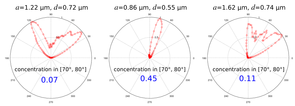
Here are results from the nonlinear optimization for three different local optima found in the search space. Each run took approximately 10 iterations to converge. The polar plot of the far-field energy density is shown for each design. Also shown is the concentration in the angular cone (objective function). The middle inset has just a single lobe in its radiation pattern and thus the highest concentration.
MPB Project #2 — Band Gap of Photonic-Crystal Nanobeam Waveguide
One-dimensional photonic-crystal waveguides consisting of a periodic array of cylindrical holes within a silicon slab of rectangular cross section are found in a wide range of applications involving lasers, optomechanics, and quantum optics. An important feature of these structures is that they can support cavity modes with low losses having quality factors typically exceeding 106 (as demonstrated in the next section) and are simpler to fabricate than their 2d or 3d counterparts. We will use MPB to compute the dispersion relation of a 1d photonic-crystal nanobeam waveguide based on the design in Applied Physics Letters, Vol. 94, No. 121106, 2009 (pdf). This structure can be fabricated using an SOI wafer.A schematic of the waveguide unit cell is shown in the figure below. The lattice periodicity (a) is 0.43 μm and the waveguide width (w) and height (h) are 0.50 and 0.22 μm. The hole radius 0.28a which is 0.12 μm. Given the 1d periodicity, we compute the dispersion relation within the irreducible Brillouin zone which spans axial wavevectors along the X direction from 0 to π/a. This is shown in the figure below. There is a bandgap, a region in which there are no guided modes, in the wavelength range of 1.30-1.70 μm. The light line of air is also shown.
import meep as mp
from meep import mpb

resolution = 20  # pixels/a

a = 0.43         # units of um
r = 0.12         # units of um
h = 0.22         # units of um
w = 0.50         # units of um

r = r/a          # units of "a"
h = h/a          # units of "a"
w = w/a          # units of "a"

nSi = 3.5
Si = mp.Medium(index=nSi)

geometry_lattice = mp.Lattice(size=mp.Vector3(1,4,4))

geometry = [ mp.Block(center=mp.Vector3(), size=mp.Vector3(mp.inf,w,h), material=Si),
             mp.Cylinder(center=mp.Vector3(), radius=r, height=mp.inf, material=mp.air) ]

num_k = 20
k_points = mp.interpolate(num_k, [mp.Vector3(0,0,0), mp.Vector3(0.5,0,0)])

num_bands = 5

ms = mpb.ModeSolver(geometry_lattice=geometry_lattice,
                    geometry=geometry,
                    k_points=k_points,
                    resolution=resolution,
                    num_bands=num_bands)

ms.run_yodd_zeven()
We run the simulation script from the shell terminal, pipe the results to a file, and then grep the relevant contents into a separate file for plotting. This takes a few seconds on a machine with a single 2.8 GHz AMD Opteron processor.
python3 nanobeam-modes.py |tee modes.out;

grep zevenyoddfreqs: modes.out |cut -d , -f3,7- |sed 1d > modes.dat;
Finally, we plot the results using matplotlib.
from numpy import *
import matplotlib.pyplot as plt

f = genfromtxt("modes.dat", delimiter=",")
plt.plot(f[:,0],f[:,1:],'b-',f[:,0],f[:,0],'k-')
plt.xlabel("wavevector k_x (units of 2π/a)")
plt.ylabel("frequency (units of 2πc/a)")
plt.axis([0,0.5,0,0.4])
plt.xticks([t for t in np.arange(0,0.6,0.1)])
plt.yticks([t for t in np.arange(0,0.5,0.1)])
plt.show()
Files: Simulation Script, Shell Launch Script, Plot Results. [gzipped tarball]
Meep Project #3 — Resonant Modes of a Photonic-Crystal Nanobeam Cavity
Using the nanobeam waveguide design of the previous section which has a bandgap between 1.30 and 1.70 μm, we proceed to create a resonant cavity by linearly tapering the lattice periodicity from a starting value ofa-start to ending a-end with radii r=0.28a of several holes on either side of a defect as shown in the schematic below. This cavity design is based on the Applied Physics Letters reference from above. We use Meep to design the cavity structure to maximize the quality factor (Q) of the fundamental resonant mode. In this example, there is only one design parameter: the cavity length (s-cav).
import meep as mp
import argparse

def main(args):

    resolution = 40                       # pixels/um

    a_start = args.a_start                # starting periodicity
    a_end = args.a_end                    # ending periodicity
    s_cav = args.s_cav                    # cavity length
    r = args.r                            # hole radius  (units of a)
    h = args.hh                           # waveguide height
    w = args.w                            # waveguide width

    dair = 1.00                           # air padding
    dpml = 1.00                           # PML thickness

    Ndef = args.Ndef                      # number of defect periods
    a_taper = mp.interpolate(Ndef, [a_start,a_end])
    dgap = a_end-2*r*a_end

    Nwvg = args.Nwvg                      # number of waveguide periods
    sx = 2*(Nwvg*a_start+sum(a_taper))-dgap+s_cav
    sy = dpml+dair+w+dair+dpml
    sz = dpml+dair+h+dair+dpml

    cell_size = mp.Vector3(sx,sy,sz)
    boundary_layers = [mp.PML(dpml)]

    nSi = 3.45
    Si = mp.Medium(index=nSi)

    geometry = [mp.Block(material=Si, center=mp.Vector3(), size=mp.Vector3(mp.inf,w,h))]

    for mm in range(Nwvg):
        geometry.append(mp.Cylinder(material=mp.air, radius=r*a_start, height=mp.inf,
                                    center=mp.Vector3(-0.5*sx+0.5*a_start+mm*a_start,0,0)))
        geometry.append(mp.Cylinder(material=mp.air, radius=r*a_start, height=mp.inf,
                                    center=mp.Vector3(+0.5*sx-0.5*a_start-mm*a_start,0,0)))

    for mm in range(Ndef+2):
        geometry.append(mp.Cylinder(material=mp.air, radius=r*a_taper[mm], height=mp.inf,
                                    center=mp.Vector3(-0.5*sx+Nwvg*a_start+(sum(a_taper[:mm]) if mm>0 else 0)+0.5*a_taper[mm],0,0)))
        geometry.append(mp.Cylinder(material=mp.air, radius=r*a_taper[mm], height=mp.inf,
                                    center=mp.Vector3(+0.5*sx-Nwvg*a_start-(sum(a_taper[:mm]) if mm>0 else 0)-0.5*a_taper[mm],0,0)))

    lambda_min = 1.46        # minimum source wavelength
    lambda_max = 1.66        # maximum source wavelength
    fmin = 1/lambda_max
    fmax = 1/lambda_min
    fcen = 0.5*(fmin+fmax)
    df = fmax-fmin

    sources = [mp.Source(mp.GaussianSource(fcen, fwidth=df), component=mp.Ey, center=mp.Vector3())]

    symmetries = [mp.Mirror(mp.X,+1), mp.Mirror(mp.Y,-1), mp.Mirror(mp.Z,+1)]

    sim = mp.Simulation(resolution=resolution,
                        cell_size=cell_size,
                        boundary_layers=boundary_layers,
                        geometry=geometry,
                        sources=sources,
                        dimensions=3,
                        symmetries=symmetries)

    sim.run(mp.in_volume(mp.Volume(center=mp.Vector3(), size=mp.Vector3(sx,sy,0)), mp.at_end(mp.output_epsilon, mp.output_efield_y)),
            mp.after_sources(mp.Harminv(mp.Ey, mp.Vector3(), fcen, df)),
            until_after_sources=500)

if __name__ == '__main__':
    parser = argparse.ArgumentParser()
    parser.add_argument('-a_start', type=float, default=0.43, help='starting periodicity (default: 0.43 um)')
    parser.add_argument('-a_end', type=float, default=0.33, help='ending periodicity (default: 0.33 um)')
    parser.add_argument('-s_cav', type=float, default=0.146, help='cavity length (default: 0.146 um)')
    parser.add_argument('-r', type=float, default=0.28, help='hole radius (default: 0.28 um)')
    parser.add_argument('-hh', type=float, default=0.22, help='waveguide height (default: 0.22 um)')
    parser.add_argument('-w', type=float, default=0.50, help='waveguide width (default: 0.50 um)')
    parser.add_argument('-Ndef', type=int, default=3, help='number of defect periods (default: 3)')
    parser.add_argument('-Nwvg', type=int, default=8, help='number of waveguide periods (default: 8)')
    args = parser.parse_args()
    main(args)
A bash script is used to sweep the cavity length (s-cav) over the range of 0.110-0.180 μm in increments of 0.005 μm. The output is written to a file with the harminv-related information extracted to a different file for plotting. The figures below show a plot of the resonant wavelength and quality factor as a function of the cavity length. The quality factor is maximum for the design with a cavity length of 0.145 μm. These are consistent with the values reported in the reference.
#!/bin/bash

for scav in `seq 0.110 0.005 0.180`; do
    mpirun -np 2 python3 nanobeam.py -s_cav ${scav} > nanobeam_cavity_length${scav}.out;
    grep harminv0: nanobeam_cavity_length${scav}.out |cut -d , -f2,4 |grep -v frequency >> nanobeam_cavity_varylength.dat;
done;
The Ey field profile for the optimal design of the fundamental cavity mode is also shown below for two cross sections. The resonant mode is confined by the bandgap in the direction of the holes (X) and index guiding in the Y and Z directions. These images were created using matplotlib as follows:
import h5py
import numpy as np
import matplotlib.pyplot as plt

eps_h5file = h5py.File('nanobeam-eps-000040000.h5','r')
eps_data = np.array(eps_h5file['eps'])
ey_h5file = h5py.File('nanobeam-ey-000040000.h5','r')
ey_data = np.array(ey_h5file['ey'])
plt.figure(dpi=100)
plt.imshow(eps_data.transpose(), interpolation='spline36', cmap='binary')
plt.imshow(ey_data.transpose(), interpolation='spline36', cmap='RdBu', alpha=0.9)
plt.axis('off')
plt.show()
Meep Project #4 — Near-Infrared Absorption Spectra of CMOS Image Sensors
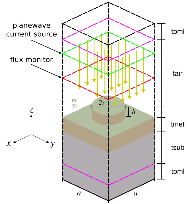
Complimentary metal oxide semiconductor (CMOS) image sensors are widely used in camera modules of mobile devices due to their lower power consumption and better electrical-readout capabilities than charge-coupled device (CCD) sensors. CMOS image sensors for visible light have recently been extended to the near infrared (IR) for applications including biomedicine, security, and chemical spectroscopy. The design challenge involves enhancing the light trapping of individual pixels at near-IR wavelengths where the absorption coefficient of silicon is small.We will investigate the back-illuminated CMOS image-sensor pixel design based on the work of Sony researchers presented in Scientific Reports, Vol. 7, No. 3832, 2017. A glass microlens (silicon dioxide) with a radius of curvature of 0.85 μm is placed on the top of the image sensor. This is necessary for focusing incident light from air into the individual pixels. A metal aperture grid made of a tungsten wire with rectangular cross section (width: 0.1 μm, height: 0.2 μm) surrounds the pixel and is placed on top of the semi-infinite crystalline-silicon substrate (thickness: 3 μm, indirect bandgap: 1.108 μm). A color filter for red, green, and blue light, which in standard designs is placed above the metal grid, is neglected in this structure. A square lattice of inverted cones on the front surface of the substrate is used to scatter the incident light in order to increase the optical path length. Deep-trench isolation is used to mitigate electrical cross talk between adjacent pixels as well as to trap photons via index guiding. This involves surrounding the pixel with a silicon-dioxide trench (width: 0.1 μm, thickness: 2 μm). A schematic of the unit-cell cross section of a single pixel is shown in the left figure below. The right figure shows the square lattice of inverted cones in the unit cell. For a broadband spectrum spanning near-IR wavelengths of 0.7 to 1.0 μm, we will use Meep to compute three device properties: (1) reflection from the top surface, (2) absorption of the tungsten wires, and (3) absorption of the silicon substrate. We will investigate the enhancement of the substrate absorption due to different lattice structures relative to a flat substrate. The design objective is to find the lattice design which maximizes the substrate absorption averaged over the entire spectrum.
The Meep simulation script has three main components: (1) defining the tungsten and silicon material parameters over the broadband wavelength spectrum, (2) setting up the supercell geometry involving a square lattice of inverted cones, and (3) computing the absorption of the metal grid and the substrate via the the total flux within these regions. The silicon material parameters are obtained by fitting the experimental values for crystalline silicon over the near-IR wavelength spectrum to a single Lorentzian-susceptibility term and adding a small imaginary component. This is explained in the supplementary-information section of Applied Physics Letters, Vol. 104, No. 091121, 2014 (pdf). All materials are included in Meep's materials library. A normally-incident planewave in air above the device is used as the source. The supercell lattice contains 3×3 unit cells with periodic boundary conditions. Four flux planes are used: one for reflection and three for transmission. The absorption is calculated as the difference in the flux entering and exiting each region (normalized by the total flux from just the source). This way, we can calculate the absorption over the entire broadband spectrum for any number of rectilinear regions using a single simulation.
import math
import argparse
import meep as mp
from meep.materials import W, SiO2, cSi

dair = 1.0                         # air gap thickness
dmcl = 1.7                         # micro lens thickness
dsub = 3.0                         # substrate thickness
dpml = 1.0                         # PML thickness

sz = dpml+dair+dmcl+dsub+dpml

lambda_min = 0.7                   # minimum source wavelength
lambda_max = 1.0                   # maximum source wavelength
fmin = 1/lambda_max
fmax = 1/lambda_min
fcen = 0.5*(fmin+fmax)
df = fmax-fmin

def main(args):
    sxy = args.Np*args.a
    cell_size = mp.Vector3(sxy,sxy,sz)

    boundary_layers = [mp.PML(dpml, direction=mp.Z, side=mp.High),
                       mp.Absorber(dpml, direction=mp.Z, side=mp.Low)]

    geometry = []

    if args.substrate:
        geometry = [mp.Sphere(material=SiO2, radius=dmcl, center=mp.Vector3(z=0.5*sz-dpml-dair-dmcl)),
                    mp.Block(material=cSi, size=mp.Vector3(mp.inf,mp.inf,dsub+dpml),
                             center=mp.Vector3(z=-0.5*sz+0.5*(dsub+dpml))),
                    mp.Block(material=W, size=mp.Vector3(mp.inf, args.wire_w, args.wire_h),
                             center=mp.Vector3(0,-0.5*sxy+0.5*args.wire_w,-0.5*sz+dpml+dsub+0.5*args.wire_h)),
                    mp.Block(material=W, size=mp.Vector3(mp.inf, args.wire_w, args.wire_h),
                             center=mp.Vector3(0,+0.5*sxy-0.5*args.wire_w,-0.5*sz+dpml+dsub+0.5*args.wire_h)),
                    mp.Block(material=W, size=mp.Vector3(args.wire_w, mp.inf, args.wire_h),
                             center=mp.Vector3(-0.5*sxy+0.5*args.wire_w,0,-0.5*sz+dpml+dsub+0.5*args.wire_h)),
                    mp.Block(material=W, size=mp.Vector3(args.wire_w, mp.inf, args.wire_h),
                             center=mp.Vector3(+0.5*sxy-0.5*args.wire_w,0,-0.5*sz+dpml+dsub+0.5*args.wire_h))]

    if args.substrate and args.texture:
        for nx in range(args.Np):
            for ny in range(args.Np):
                cx = -0.5*sxy+(nx+0.5)*args.a
                cy = -0.5*sxy+(ny+0.5)*args.a
                geometry.append(mp.Cone(material=SiO2,
                                        radius=0,
                                        radius2=args.cone_r,
                                        height=args.cone_h,
                                        center=mp.Vector3(cx,cy,0.5*sz-dpml-dair-dmcl-0.5*args.cone_h)))

    if args.substrate:
        geometry.append(mp.Block(material=SiO2,
                                 size=mp.Vector3(mp.inf, args.trench_w, args.trench_h),
                                 center=mp.Vector3(0, -0.5*sxy+0.5*args.trench_w, 0.5*sz-dpml-dair-dmcl-0.5*args.trench_h)))
        geometry.append(mp.Block(material=SiO2,
                                 size=mp.Vector3(mp.inf, args.trench_w, args.trench_h),
                                 center=mp.Vector3(0, +0.5*sxy-0.5*args.trench_w, 0.5*sz-dpml-dair-dmcl-0.5*args.trench_h)))
        geometry.append(mp.Block(material=SiO2,
                                 size=mp.Vector3(args.trench_w, mp.inf, args.trench_h),
                                 center=mp.Vector3(-0.5*sxy+0.5*args.trench_w, 0, 0.5*sz-dpml-dair-dmcl-0.5*args.trench_h)))
        geometry.append(mp.Block(material=SiO2,
                                 size=mp.Vector3(args.trench_w, mp.inf, args.trench_h),
                                 center=mp.Vector3(+0.5*sxy-0.5*args.trench_w, 0, 0.5*sz-dpml-dair-dmcl-0.5*args.trench_h)))

    sources = [mp.Source(mp.GaussianSource(fcen, fwidth=df),
                         component=mp.Ex,
                         center=mp.Vector3(z=0.5*sz-dpml-0.5*dair),
                         size=mp.Vector3(sxy,sxy))]

    sim = mp.Simulation(resolution=args.res,
                        cell_size=cell_size,
                        boundary_layers=boundary_layers,
                        geometry=geometry,
                        dimensions=3,
                        split_chunks_evenly=False,
                        k_point=mp.Vector3(),
                        sources=sources)

    nfreq = 50
    refl = sim.add_flux(fcen, df, nfreq, mp.FluxRegion(center=mp.Vector3(0,0,0.5*sz-dpml),size=mp.Vector3(sxy,sxy,0)))
    trans_grid = sim.add_flux(fcen, df, nfreq,
                              mp.FluxRegion(center=mp.Vector3(0,0,-0.5*sz+dpml+dsub+args.wire_h),size=mp.Vector3(sxy,sxy,0)))
    trans_sub_top = sim.add_flux(fcen, df, nfreq,
                                 mp.FluxRegion(center=mp.Vector3(0,0,-0.5*sz+dpml+dsub),size=mp.Vector3(sxy,sxy,0)))
    trans_sub_bot = sim.add_flux(fcen, df, nfreq,
                                 mp.FluxRegion(center=mp.Vector3(0,0,-0.5*sz+dpml),size=mp.Vector3(sxy,sxy,0)))

    sim.run(until_after_sources=mp.stop_when_fields_decayed(50, mp.Ex, mp.Vector3(z=-0.5*sz+dpml+0.5*dsub), 1e-9))

if __name__ == '__main__':
    parser = argparse.ArgumentParser()
    parser.add_argument('-res', type=float, default=30, help='reslution (default: 30 pixels/um)')
    parser.add_argument('-substrate', action='store_true', default=False, help='add the substrate? (default: False)')
    parser.add_argument('-texture', action='store_true', default=False, help='add the texture? (default: False)')
    parser.add_argument('-a', type=float, default=0.4, help='lattice periodicity (default: 0.4 um)')
    parser.add_argument('-cone_r', type=float, default=0.2, help='cone radius (default: 0.2 um)')
    parser.add_argument('-cone_h', type=float, default=0.28247, help='cone height (default: 0.28247 um)')
    parser.add_argument('-wire_w', type=float, default=0.1, help='metal-grid wire width (default: 0.1 um)')
    parser.add_argument('-wire_h', type=float, default=0.2, help='metal-grid wire height (default: 0.2 um)')
    parser.add_argument('-trench_w', type=float, default=0.1, help='trench width (default: 0.1 um)')
    parser.add_argument('-trench_h', type=float, default=2.0, help='trench height (default: 2.0 um)')
    parser.add_argument('-Np', type=int, default=3, help='number of periods in supercell (default: 3)')
    args = parser.parse_args()
    main(args)
We will create a Bash shell script to run three simulations for each lattice design: (1) the empty cell with just the source, (2) the flat substrate, and (3) the textured substrate. The lattice periodicity (a) is varied over the range of 0.40 to 0.70 μm. The simulation output is piped to a file for post processing in Python.
#!/bin/bash

for a in `seq 0.40 0.02 0.70`; do
    mpirun -np 4 python3 cmos_sensor.py -a ${a} > cmos_a${a}_empty.out;
    grep flux1: cmos_a${a}_empty.out |cut -d , -f2- > cmos_a${a}_empty.dat;

    mpirun -np 4 python3 cmos_sensor.py -a ${a} -substrate > cmos_a${a}_flat.out;
    grep flux1: cmos_a${a}_flat.out |cut -d , -f2- > cmos_a${a}_flat.dat;

    mpirun -np 4 python3 cmos_sensor.py -a ${a} -substrate -texture > cmos_a${a}_texture.out;
    grep flux1: cmos_a${a}_texture.out |cut -d , -f2- > cmos_a${a}_texture.dat;
done;
The left figure below is a contour plot of the substrate absorption as a function of wavelength and lattice periodicity. This is the fraction of the incident light which is absorbed by just the crystalline-silicon substrate. For all lattice designs, the absorption is largest at the smallest wavelengths which is expected. The right figure shows the enhancement of the substrate absorption due to the lattice relative to a flat substrate (i.e., no lattice). The lattice produces wavelength-dependent scattering effects which can be seen as the dark spots in the contour plot.
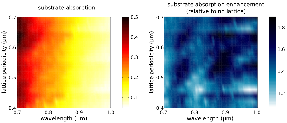
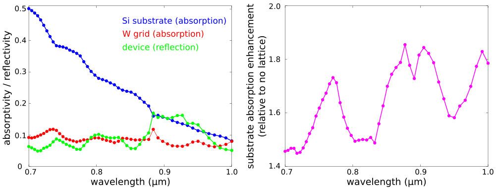
The optimal lattice design which has the largest average absorption over the broadband spectrum is a=0.64 μm with 24.5%±12.2%. A plot of the substrate and grid absorption as well as the reflection from the device for this lattice design are shown in the left figure below. For comparison, the average substrate absorption for the no-lattice reference design is 15.4%±8.5%. The optimal lattice yields an average enhancement per wavelength of 1.6±0.6.
Files: Simulation Script, Shell Launch Script, Plot Results. [gzipped tarball]
Meep Project #5 — Thermal Radiation Spectra of Plasmonic Metamaterials
We can use Meep to compute the thermal-radiation spectra of metallic devices. This is based on Kirchhoff's law of thermal radiation which states that for an arbitrary body emitting and absorbing thermal radiation in thermodynamic equilibrium, the emissivity is equal to the absorptivity. Computing the emissivity (or emittance) of the device is therefore equivalent to computing its absorptivity (or absorptance). The thermal radiation spectra of the device is the product of its absorptance with the black body radiation spectrum given by Planck's law.The schematic below shows the unit cell geometry of a plasmonic metamaterial. The design is based on J. Optical Society of America B, Vol. 30, pp. 165-172, 2013. The structure consists of a square lattice of cylindrical Platinum (Pt) rods on top of a semi-infinite silicon substrate. In a real experiment, Joule or Convective heating would be applied to the Pt layer and the thermal radiation measured using an infrared camera. In the simulation, a planewave is normally incident from the air region above the device. Periodic boundary conditions are used in the xy plane and perfectly-matched layers (PMLs) in the transverse z direction. The absorptance can be obtained as simply 1-reflectance, using a single flux monitor as shown in the schematic. There is no transmission through the Pt layer into the substrate since the incident planewave is either reflected from the device or absorbed by surface-plasmon polaritons.
The design objective, for applications such as sensing, is to find a lattice geometry which has a single emission peak with minimum bandwidth and maximum amplitude in the near-infrared wavelength range (i.e., 2-5 μm). There are two degrees of freedom: the lattice periodicity (a) and rod radius (r). The rod height (h) is fixed. Given the small number of parameters, we can explore the entire design space using a brute-force search. The simulation script, shell launch script, and sample results are shown below.
import meep as mp
import math
import cmath
import argparse

def main(args):

    # default unit length is 1 um
    um_scale = 1.0

    # conversion factor for eV to 1/um [=1/hc]
    eV_um_scale = um_scale/1.23984193

    # Pt from A.D. Rakic et al., Applied Optics, Vol. 37, No. 22, pp. 5271-83, 1998
    Pt_plasma_frq = 9.59*eV_um_scale
    Pt_f0 = 0.333
    Pt_frq0 = 1e-10
    Pt_gam0 = 0.080*eV_um_scale
    Pt_sig0 = Pt_f0*Pt_plasma_frq**2/Pt_frq0**2
    Pt_f1 = 0.191
    Pt_frq1 = 0.780*eV_um_scale      # 1.590 um
    Pt_gam1 = 0.517*eV_um_scale
    Pt_sig1 = Pt_f1*Pt_plasma_frq**2/Pt_frq1**2
    Pt_f2 = 0.659
    Pt_frq2 = 1.314*eV_um_scale      # 0.944 um
    Pt_gam2 = 1.838*eV_um_scale
    Pt_sig2 = Pt_f2*Pt_plasma_frq**2/Pt_frq2**2

    Pt_susc = [ mp.DrudeSusceptibility(frequency=Pt_frq0, gamma=Pt_gam0, sigma=Pt_sig0),
                mp.LorentzianSusceptibility(frequency=Pt_frq1, gamma=Pt_gam1, sigma=Pt_sig1),
                mp.LorentzianSusceptibility(frequency=Pt_frq2, gamma=Pt_gam2, sigma=Pt_sig2) ]

    Pt = mp.Medium(epsilon=1.0, E_susceptibilities=Pt_susc)

    resolution = 40     # pixels/um

    a = args.aa         # lattice periodicity
    r = args.rr         # metal rod radius
    h = 0.2             # metal rod height
    tmet = 0.3          # metal layer thickness
    tsub = 2.0          # substrate thickness
    tabs = 5.0          # PML thickness
    tair = 4.0          # air thickness

    sz = tabs+tair+h+tmet+tsub+tabs
    cell_size = mp.Vector3(a,a,sz)

    pml_layers = [mp.PML(thickness=tabs,direction=mp.Z,side=mp.High),
                  mp.Absorber(thickness=tabs,direction=mp.Z,side=mp.Low)]

    lmin = 2.0          # source min wavelength
    lmax = 5.0          # source max wavelength
    fmin = 1/lmax       # source min frequency
    fmax = 1/lmin       # source max frequency
    fcen = 0.5*(fmin+fmax)
    df = fmax-fmin

    nSi = 3.5
    Si = mp.Medium(index=nSi)

    if args.empty:
        geometry = []
    else:
        geometry = [ mp.Cylinder(material=Pt, radius=r, height=h, center=mp.Vector3(0,0,0.5*sz-tabs-tair-0.5*h)),
                     mp.Block(material=Pt, size=mp.Vector3(mp.inf,mp.inf,tmet),
                              center=mp.Vector3(0,0,0.5*sz-tabs-tair-h-0.5*tmet)),
                     mp.Block(material=Si, size=mp.Vector3(mp.inf,mp.inf,tsub+tabs),
                              center=mp.Vector3(0,0,0.5*sz-tabs-tair-h-tmet-0.5*(tsub+tabs))) ]

    # CCW rotation angle (degrees) about Y-axis of PW current source; 0 degrees along -z axis
    theta = math.radians(args.theta)

    # k with correct length (plane of incidence: XZ)
    k = mp.Vector3(math.sin(theta),0,math.cos(theta)).scale(fcen)

    def pw_amp(k, x0):
        def _pw_amp(x):
            return cmath.exp(1j * 2 * math.pi * k.dot(x + x0))
        return _pw_amp

    src_pos = 0.5*sz-tabs-0.2*tair
    sources = [ mp.Source(mp.GaussianSource(fcen, fwidth=df), component=mp.Ey, center=mp.Vector3(0,0,src_pos),
                          size=mp.Vector3(a,a,0),
                          amp_func=pw_amp(k, mp.Vector3(0,0,src_pos))) ]

    sim = mp.Simulation(cell_size=cell_size,
                        geometry=geometry,
                        sources=sources,
                        boundary_layers=pml_layers,
                        k_point = k,
                        resolution=resolution)

    nfreq = 50
    refl = sim.add_flux(fcen, df, nfreq, mp.FluxRegion(center=mp.Vector3(0,0,+0.5*sz-tabs-0.5*tair),size=mp.Vector3(a,a,0)))

    if not args.empty:
        sim.load_minus_flux('refl-flux', refl)

    sim.run(until_after_sources=mp.stop_when_fields_decayed(25, mp.Ey, mp.Vector3(0,0,0.5*sz-tabs-0.5*tair), 1e-7))

    if args.empty:
        sim.save_flux('refl-flux', refl)

    sim.display_fluxes(refl)

if __name__ == '__main__':
    parser = argparse.ArgumentParser()
    parser.add_argument('-empty', action='store_true', default=False, help="empty? (default: False)")
    parser.add_argument('-aa', type=float, default=4.5, help='lattice periodicity (default: 4.5 um)')
    parser.add_argument('-rr', type=float, default=1.5, help='Pt rod radius (default: 1.5 um)')
    parser.add_argument('-theta', type=float, default=0, help='angle of planewave current source (default: 0 degrees)')
    args = parser.parse_args()
    main(args)
#!/bin/bash

np=20;

for a in `seq 4.1 0.1 5.0`; do
    mpirun -np ${np} python3 -u emitter.py -empty -aa {a} > flux0_a${a}.out;
    grep flux1: flux0_a${a}.out |cut -d , -f2- > flux0_a${a}.dat;
    for r_frac in `seq 0.1 0.1 0.4`; do
        r=$(printf "%0.2f" `echo "${a}*${r_frac}" |bc`);
        mpirun -np ${np} python3 -u emitter.py -aa ${a} -rr ${r} > flux_a${a}_r${r}.out;
        grep flux1: flux_a${a}_r${r}.out |cut -d , -f2- > flux_a${a}_r${r}.dat;
    done;
done;
Note that this emissivity calculation is for the thermal radiation directed in the upward direction. To compute the thermal radiation in the downward direction (which is mainly considered loss), we would need to do a separate calculation to obtain the emissivity in the downward direction. This would involve sending a planewave from the bottom of the computational cell and computing the absorptance using the same approach involving the reflectance. The fraction of the total radiation which is directed upward is then the ratio of the emissivity in the upward direction over the sum of the emissivities in the upward and downward directions.
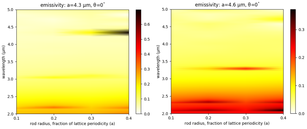
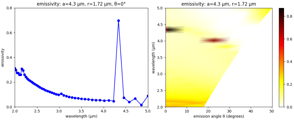
We can also compute the thermal radiation spectra at an oblique angle θ. This is given by equation 63.24 on page 189 of Statistical Physics, Third Edition, 1980 by L.D. Landau and E.M. Lifshitz as: e'(λ)cos(θ)A(λ,θ), where e'(λ) is the black body emission spectrum and A(λ,θ) is the absorptance. We compute the angular radiation spectra cos(θ)A(λ,θ) in the range [0°, 30°] for the metamaterial design with a=4.3 μm and r=1.72 μm. This structure has a single, narrowband emissivity peak of nearly 0.8 at a wavelength of 4.4 μm which is shown in the left figure below.
The following are the shell launch script and plotting script.
#!/bin/bash

np=20;

a=4.3;
r=1.72;

for t in `seq 0 5 30`; do
    mpirun -np ${np} python3 -u emitter.py -empty -aa ${a} -theta ${t} > flux0_a${a}_theta${t}.out;
    grep flux1: flux0_a${a}_theta${t}.out |cut -d , -f2- > flux0_a${a}_theta${t}.dat;

    mpirun -np ${np} python3 -u emitter.py -aa ${a} -rr ${r} -theta ${t} > flux_a${a}_r${r}_theta${t}.out;
    grep flux1: flux_a${a}_r${r}_theta${t}.out |cut -d , -f2- > flux_a${a}_r${r}_theta${t}.dat;
done;
import matplotlib.pyplot as plt
import numpy as np
import numpy.matlib
import math

lmin = 2.0          # source min wavelength
lmax = 5.0          # source max wavelength
fmin = 1/lmax       # source min frequency
fmax = 1/lmin       # source max frequency
fcen = 0.5*(fmin+fmax)

thetas = range(0,35,5)
kx = [fcen*math.sin(t) for t in [math.radians(float(t)) for t in thetas]]
Refl = np.empty((50,thetas.size))
Abs = np.empty((50,thetas.size))
theta_out = np.empty((50,thetas.size))

for k in range(thetas.size):
    f0 = np.genfromtxt("flux0_a4.3_theta{}.dat".format(thetas[k]), delimiter=",")
    f = np.genfromtxt("flux_a4.3_r1.72_theta{}.dat".format(thetas[k]), delimiter=",")
    Refl[:,k] = -f[:,1]/f0[:,1]
    theta_out[:,k] = np.asarray([math.degrees(math.asin(kx[k]/f0[j,0])) for j in range(50)])
    Abs[:,k] = np.asarray([(1-Refl[j,k])*math.cos(math.radians(theta_out[j,k])) for j in range(50)])

Abs[Abs<0] = 0
wvl = 1/f0[:,0]
wvls = np.matlib.repmat(np.reshape(wvl,(wvl.size,1)),1,thetas.size)

plt.figure(dpi=100)
plt.pcolormesh(theta_out, wvls, Abs, cmap='hot_r', shading='gouraud', vmin=0, vmax=Abs.max())
plt.axis([theta_out.min(), theta_out.max(), wvl[-1], wvl[0]])
plt.xlabel("emission angle (degrees)")
plt.xticks([t for t in range(0,60,10)])
plt.ylabel("wavelength (um)")
plt.yticks([t for t in np.arange(2.0,5.5,0.5)])
plt.title(r"emissivity: a=4.3 um, r=1.72 um")
cbar = plt.colorbar()
cbar.set_ticks([t for t in np.arange(0,1.0,0.2)])
cbar.set_ticklabels(["{:.1f}".format(t) for t in np.arange(0,1.0,0.2)])
plt.show()
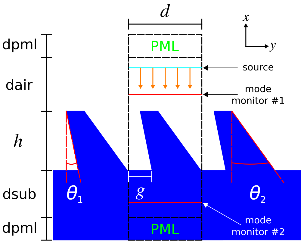
Meep Project #6 — Bidirectional Scattering Distribution Function (BSDF) of Asymmetric Gratings
In this example, we use Meep to compute the bidirectional scattering distribution function (BSDF) of a diffraction grating. BSDFs are used in ray tracing for physically based rendering of textured surfaces with wavelength or sub-wavelength (i.e., micro- or nano-scale) features. The BSDF of a grating involves computing the reflectance and transmittance at a single wavelength for all possible diffraction orders (or "rays") for an incident planewave source over a range of angles. This calculation is similar to the Meep tutorial example for a binary grating.The asymmetric grating design, shown in the schematic below along with the overall simulation geometry, is based on Optics Express, Vol. 15, pp. 2067-74, 2007. The unit cell has five degrees of freedom: periodicity (d), height (h), gap (g), and two angles for the side walls (θ1 and θ2). These have arbitrary default values of 3.5 μm, 1.9 μm, 0.7 μm, 12.8°, and 27.4°. The grating material is episulfide with a wavelength-independent refractive index of 1.716. A planewave pulse centered at 0.5 μm is incident from the air region above the grating. The planewave's angle and polarization are specified using the
src_angle and src_pol command-line parameters. Two mode monitors are used to compute the reflectance and transmittance of the diffracted orders via mode decomposition. Note that for any polarized planewave at normal incidence, the asymmetric grating yields diffraction orders which are either even or odd. To separate these modes in the output, we must invoke get_eigenmode_coefficients twice with its eig_parity parameter set to EVEN_Y or ODD_Y. The reflectance and transmittance of each diffracted order is output on separate lines, including its angle, prefixed by refl: and tran:. At the end of the simulation, the total reflectance and transmittance are output on the line prefixed by total:.
import math
import cmath
import numpy as np
import argparse
import sys
import meep as mp

def main(args):
  resolution = args.res  # pixels/μm

  dpml = 1.0             # PML length
  dair = 4.0             # padding length between PML and grating
  dsub = 3.0             # substrate thickness
  d = args.dd            # grating period
  h = args.hh            # grating height
  g = args.gg            # grating gap
  theta_1 = math.radians(args.theta_1)  # grating sidewall angle #1
  theta_2 = math.radians(args.theta_2)  # grating sidewall angle #2

  sx = dpml+dair+h+dsub+dpml
  sy = d

  cell_size = mp.Vector3(sx,sy,0)
  pml_layers = [mp.Absorber(thickness=dpml,direction=mp.X)]

  wvl = 0.5              # center wavelength
  fcen = 1/wvl           # center frequency
  df = 0.05*fcen         # frequency width

  ng = 1.716             # episulfide refractive index @ 0.532 μm
  glass = mp.Medium(index=ng)

  if args.src_pol == 1:
    src_cmpt = mp.Ez
    eig_parity = mp.ODD_Z
  elif args.src_pol == 2:
    src_cmpt = mp.Hz
    eig_parity = mp.EVEN_Z
  else:
    sys.exit("error: src_pol={} is invalid".format(args.src_pol))

  # rotation angle of incident planewave source; CCW about Z axis, 0 degrees along +X axis
  theta_src = math.radians(args.src_angle)

  # k (in source medium) with correct length (plane of incidence: XY)
  k = mp.Vector3(math.cos(theta_src),math.sin(theta_src),0).scale(fcen)
  if theta_src == 0:
    k = mp.Vector3(0,0,0)

  def pw_amp(k,x0):
    def _pw_amp(x):
      return cmath.exp(1j*2*math.pi*k.dot(x+x0))
    return _pw_amp

  src_pt = mp.Vector3(-0.5*sx+dpml+0.2*dair,0,0)
  sources = [mp.Source(mp.GaussianSource(fcen,fwidth=df),
                       component=src_cmpt,
                       center=src_pt,
                       size=mp.Vector3(0,sy,0),
                       amp_func=pw_amp(k,src_pt))]

  sim = mp.Simulation(resolution=resolution,
                      cell_size=cell_size,
                      boundary_layers=pml_layers,
                      k_point=k,
                      sources=sources)

  refl_pt = mp.Vector3(-0.5*sx+dpml+0.7*dair,0,0)
  refl_flux = sim.add_flux(fcen, 0, 1, mp.FluxRegion(center=refl_pt, size=mp.Vector3(0,sy,0)))

  sim.run(until_after_sources=100)

  input_flux = mp.get_fluxes(refl_flux)
  input_flux_data = sim.get_flux_data(refl_flux)

  sim.reset_meep()

  geometry = [mp.Block(material=glass, size=mp.Vector3(dpml+dsub,mp.inf,mp.inf), center=mp.Vector3(0.5*sx-0.5*(dpml+dsub),0,0)),
              mp.Prism(material=glass,
                       height=mp.inf,
                       vertices=[mp.Vector3(0.5*sx-dpml-dsub,0.5*sy,0),
                                 mp.Vector3(0.5*sx-dpml-dsub-h,0.5*sy-h*math.tan(theta_2),0),
                                 mp.Vector3(0.5*sx-dpml-dsub-h,-0.5*sy+g-h*math.tan(theta_1),0),
                                 mp.Vector3(0.5*sx-dpml-dsub,-0.5*sy+g,0)])]

  sim = mp.Simulation(resolution=resolution,
                      cell_size=cell_size,
                      boundary_layers=pml_layers,
                      k_point=k,
                      sources=sources,
                      geometry=geometry)

  refl_flux = sim.add_flux(fcen, 0, 1, mp.FluxRegion(center=refl_pt, size=mp.Vector3(0,sy,0)))
  sim.load_minus_flux_data(refl_flux, input_flux_data)

  tran_pt = mp.Vector3(0.5*sx-dpml-0.5*dsub,0,0)
  tran_flux = sim.add_flux(fcen, 0, 1, mp.FluxRegion(center=tran_pt, size=mp.Vector3(0,sy,0)))

  sim.run(until_after_sources=500)

  kdom_tol = 1e-2
  angle_tol = 1e-6

  Rsum = 0
  Tsum = 0
  if theta_src == 0:
    nm_r = int(0.5*(np.floor((fcen-k.y)*d)-np.ceil((-fcen-k.y)*d)))       # number of reflected orders

    res = sim.get_eigenmode_coefficients(refl_flux, range(1,nm_r+1), eig_parity=eig_parity+mp.EVEN_Y)
    r_coeffs = res.alpha
    r_kdom = res.kdom
    for nm in range(nm_r):
      if r_kdom[nm].x > kdom_tol:
        r_angle = np.sign(r_kdom[nm].y)*math.acos(r_kdom[nm].x/fcen) if (r_kdom[nm].x % fcen > angle_tol) else 0
        Rmode = abs(r_coeffs[nm,0,1])**2/input_flux[0]
        print("refl: (even_y), {}, {:.2f}, {:.8f}".format(nm,math.degrees(r_angle),Rmode))
        Rsum += Rmode

    res = sim.get_eigenmode_coefficients(refl_flux, range(1,nm_r+1), eig_parity=eig_parity+mp.ODD_Y)
    r_coeffs = res.alpha
    r_kdom = res.kdom
    for nm in range(nm_r):
      if r_kdom[nm].x > kdom_tol:
        r_angle = np.sign(r_kdom[nm].y)*math.acos(r_kdom[nm].x/fcen) if (r_kdom[nm].x % fcen > angle_tol) else 0
        Rmode = abs(r_coeffs[nm,0,1])**2/input_flux[0]
        print("refl: (odd_y), {}, {:.2f}, {:.8f}".format(nm,math.degrees(r_angle),Rmode))
        Rsum += Rmode

    nm_t = int(0.5*(np.floor((fcen*ng-k.y)*d)-np.ceil((-fcen*ng-k.y)*d))) # number of transmitted orders

    res = sim.get_eigenmode_coefficients(tran_flux, range(1,nm_t+1), eig_parity=eig_parity+mp.EVEN_Y)
    t_coeffs = res.alpha
    t_kdom = res.kdom
    for nm in range(nm_t):
      if t_kdom[nm].x > kdom_tol:
        t_angle = np.sign(t_kdom[nm].y)*math.acos(t_kdom[nm].x/(ng*fcen)) if (t_kdom[nm].x % ng*fcen > angle_tol) else 0
        Tmode = abs(t_coeffs[nm,0,0])**2/input_flux[0]
        print("tran: (even_y), {}, {:.2f}, {:.8f}".format(nm,math.degrees(t_angle),Tmode))
        Tsum += Tmode

    res = sim.get_eigenmode_coefficients(tran_flux, range(1,nm_t+1), eig_parity=eig_parity+mp.ODD_Y)
    t_coeffs = res.alpha
    t_kdom = res.kdom
    for nm in range(nm_t):
      if t_kdom[nm].x > kdom_tol:
        t_angle = np.sign(t_kdom[nm].y)*math.acos(t_kdom[nm].x/(ng*fcen)) if (t_kdom[nm].x % ng*fcen > angle_tol) else 0
        Tmode = abs(t_coeffs[nm,0,0])**2/input_flux[0]
        print("tran: (odd_y), {}, {:.2f}, {:.8f}".format(nm,math.degrees(t_angle),Tmode))
        Tsum += Tmode
  else:
    nm_r = int(np.floor((fcen-k.y)*d)-np.ceil((-fcen-k.y)*d))       # number of reflected orders
    res = sim.get_eigenmode_coefficients(refl_flux, range(1,nm_r+1), eig_parity=eig_parity)
    r_coeffs = res.alpha
    r_kdom = res.kdom
    for nm in range(nm_r):
      if r_kdom[nm].x > kdom_tol:
        r_angle = np.sign(r_kdom[nm].y)*math.acos(r_kdom[nm].x/fcen) if (r_kdom[nm].x % fcen > angle_tol) else 0
        Rmode = abs(r_coeffs[nm,0,1])**2/input_flux[0]
        print("refl:, {}, {:.2f}, {:.8f}".format(nm,math.degrees(r_angle),Rmode))
        Rsum += Rmode

    nm_t = int(np.floor((fcen*ng-k.y)*d)-np.ceil((-fcen*ng-k.y)*d)) # number of transmitted orders
    res = sim.get_eigenmode_coefficients(tran_flux, range(1,nm_t+1), eig_parity=eig_parity)
    t_coeffs = res.alpha
    t_kdom = res.kdom
    for nm in range(nm_t):
      if t_kdom[nm].x > kdom_tol:
        t_angle = np.sign(t_kdom[nm].y)*math.acos(t_kdom[nm].x/(ng*fcen)) if (t_kdom[nm].x % ng*fcen > angle_tol) else 0
        Tmode = abs(t_coeffs[nm,0,0])**2/input_flux[0]
        print("tran:, {}, {:.2f}, {:.8f}".format(nm,math.degrees(t_angle),Tmode))
        Tsum += Tmode

  print("total:, {:.6f}, {:.6f}, {:.6f}".format(Rsum,Tsum,Rsum+Tsum))

if __name__ == '__main__':
  parser = argparse.ArgumentParser()
  parser.add_argument('-res', type=int, default=50, help='resolution (default: 50 pixels/μm)')
  parser.add_argument('-src_pol', type=int, default=1, help='source polarization (1: Ez, 2: Hz, default: Ez)')
  parser.add_argument('-src_angle', type=float, default=0, help='source angle (default: 0 degrees)')
  parser.add_argument('-dd', type=float, default=3.5, help='grating periodicity (default: 3.5 μm)')
  parser.add_argument('-gg', type=float, default=1.9, help='grating gap (default: 1.9 μm)')
  parser.add_argument('-hh', type=float, default=0.7, help='grating height (default: 0.7 μm)')
  parser.add_argument('-theta_1', type=float, default=12.8, help='grating sidewall angle #1 (default: 12.8 degrees)')
  parser.add_argument('-theta_2', type=float, default=27.4, help='grating sidewall angle #2 (default: 27.4 degrees)')
  args = parser.parse_args()
  main(args)
The following Bash script executes the grating BSDF simulation for both polarizations over the angular range of -45° to +45° in increments of 5°. The output of each run is piped to a file. The data for the total reflectance and transmittance is collected in separate files for each polarization.
#!/bin/bash

d=3.5
h=1.9
g=0.7

for t in `seq -45 5 45`; do
    python grating.py -src_pol 1 -src_angle ${t} -dd ${d} -hh ${h} -gg ${g} |tee grating_d${d}_h${h}_g${g}_Ez_theta${t}.out;
    grep total: grating_d${d}_h${h}_g${g}_Ez_theta${t}.out |cut -d , -f2- >> grating_Ez_d${d}_h${h}_g${g}.dat;

    python grating.py -src_pol 2 -src_angle ${t} -dd ${d} -hh ${h} -gg ${g} |tee grating_d${d}_h${h}_g${g}_Hz_theta${t}.out;
    grep total: grating_d${d}_h${h}_g${g}_Hz_theta${t}.out |cut -d , -f2- >> grating_Hz_d${d}_h${h}_g${g}.dat;
done
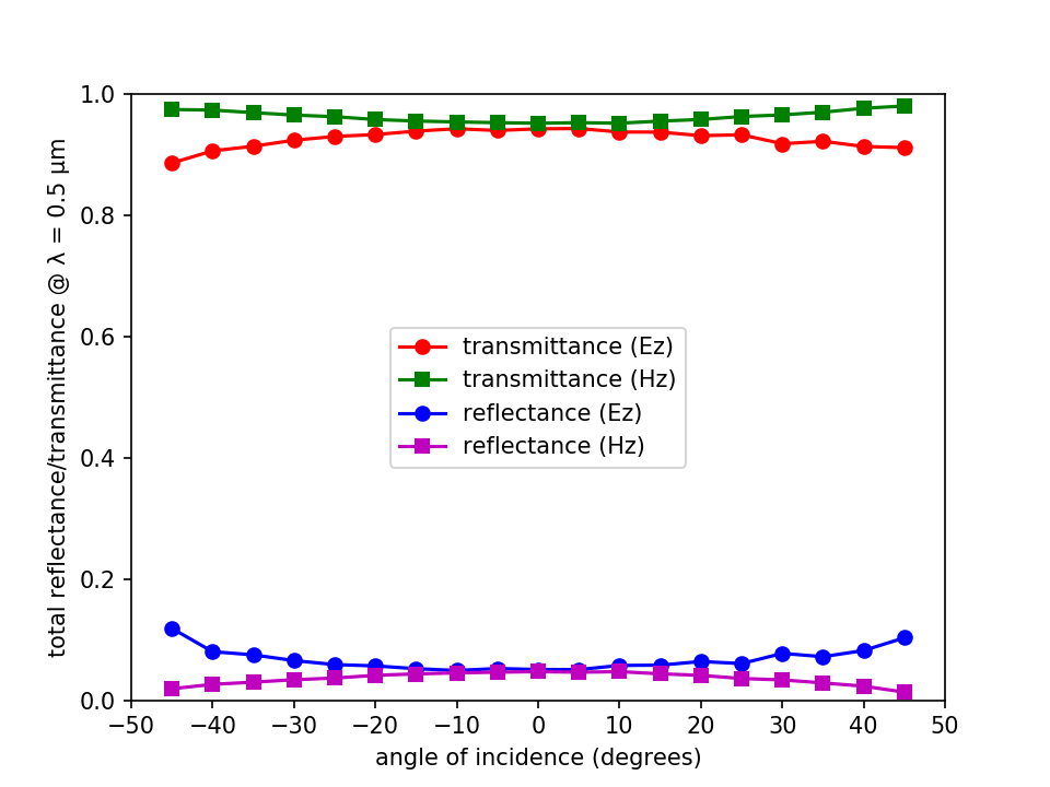
The Python script below plots the reflectance and transmittance spectra.
import matplotlib.pyplot as plt
import numpy as np

thetas = range(-45,50,5)
ez_data = np.genfromtxt('grating_Ez_d3.5_h1.9_g0.7.dat',delimiter=',')
hz_data = np.genfromtxt('grating_Hz_d3.5_h1.9_g0.7.dat',delimiter=',')

plt.figure(dpi=150)
plt.plot(thetas,ez_data[:,1],'ro-',clip_on=False,label='transmittance (Ez)')
plt.plot(thetas,hz_data[:,1],'gs-',clip_on=False,label='transmittance (Hz)')
plt.plot(thetas,ez_data[:,0],'bo-',clip_on=False,label='reflectance (Ez)')
plt.plot(thetas,hz_data[:,0],'ms-',clip_on=False,label='reflectance (Hz)')
plt.axis([-50,50,0,1])
plt.xticks([t for t in range(-50,60,10)])
plt.yticks([t for t in np.arange(0,1.2,0.2)])
plt.legend(loc="center")
plt.xlabel("angle of incidence (degrees)")
plt.ylabel("total reflectance/transmittance @ λ = 0.5 μm")
plt.show()
The following is the output for the reflected orders for an Ez-polarized source at an incident angle of +25°. The first numerical column is the diffraction order (an integer), the second is the angle of the mode (in degrees), and the third is the reflectance. The sign of the angles refers to the direction of rotation about the Z axis: clockwise (+) or counter-clockwise (-) with 0° along the -X direction.
 0, -0.32, 0.00011259
 1, 7.89, 0.00171405
 2, -8.54, 0.00119997
 3, 16.26, 0.00873309
 4, -16.94, 0.00113014
 5, 25.02, 0.03593260
 6, -25.73, 0.00078624
 7, 34.46, 0.00636958
 8, -35.24, 0.00071590
 9, 45.13, 0.00041392
 10, -46.05, 0.00038857
 11, 58.38, 0.00160692
 12, -59.63, 0.00017113
Shown below is the output for the transmitted orders. Note that the fifth diffraction order at 14.27° has a transmittance of nearly 0.51. This indicates that 51% of the input power is directed into just a single mode. An application of this type of calculation for display applications would involve maximizing the reflectance or transmittance of a given diffraction order.
 0, -0.19, 0.03480129
 1, 4.59, 0.02409643
 2, -4.96, 0.00130120
 3, 9.39, 0.02907887
 4, -9.78, 0.05293424
 5, 14.27, 0.50628602
 6, -14.66, 0.02359082
 7, 19.25, 0.05468124
 8, -19.65, 0.00661593
 9, 24.39, 0.00175412
 10, -24.81, 0.01615384
 11, 29.75, 0.02172649
 12, -30.18, 0.00517371
 13, 35.41, 0.03408556
 14, -35.88, 0.00400024
 15, 41.51, 0.00015972
 16, -42.01, 0.00049539
 17, 48.24, 0.01024240
 18, -48.81, 0.00154459
 19, 56.02, 0.01787368
 20, -56.70, 0.00272488
 21, 65.85, 0.07193458
 22, -66.79, 0.00265052
Finally, the plot below shows the total reflectance and transmittance (i.e., sum of all the diffraction orders) for both polarizations as a function of the angle of incidence of the planewave source. Due to the relatively low index of the grating, most of the input power is transmitted. Additionally, coherent scattering effects are weak which is why there is little variation in the results with the source angle and polarization. The intrinsic asymmetry of the grating design is verified by the asymmetry in the results for positive and negative angles.